| Part No.: | LTC2266-14 |
| Page: | 32 Pages |
| Size: | 644 KB |
| Manufacturer: | Linear Technology |
| Logo: |  |
| Views: | 1 |
| Update Time: | 2024-11-21 10:55:58 |
| DataSheet: | Download |
| Part No. | Packing | SPQ | Marking | MSL | Pins | Temp Range | Package Description | Buy |
| LTC2266CUJ-14#PBF | Tube | 61 | LTC2266UJ-14 | 1 | 40 | 0°C ~70°C | 40-Lead (6mm × 6mm) Plastic QFN | |
| LTC2266CUJ-14#TRPBF | Reel | 2000 | LTC2266UJ-14 | 1 | 40 | 0°C ~70°C | 40-Lead (6mm × 6mm) Plastic QFN | |
| LTC2266CUJ-14#TRMPBF | Reel | 500 | LTC2266UJ-14 | 1 | 40 | 0°C ~70°C | 40-Lead (6mm × 6mm) Plastic QFN | |
| LTC2266IUJ-14#PBF | Tube | 61 | LTC2266UJ-14 | 1 | 40 | -40°C ~85°C | 40-Lead (6mm × 6mm) Plastic QFN | |
| LTC2266IUJ-14#TRPBF | Reel | 2000 | LTC2266UJ-14 | 1 | 40 | -40°C ~85°C | 40-Lead (6mm × 6mm) Plastic QFN | |
| LTC2266IUJ-14#TRMPBF | Reel | 500 | LTC2266UJ-14 | 1 | 40 | -40°C ~85°C | 40-Lead (6mm × 6mm) Plastic QFN |
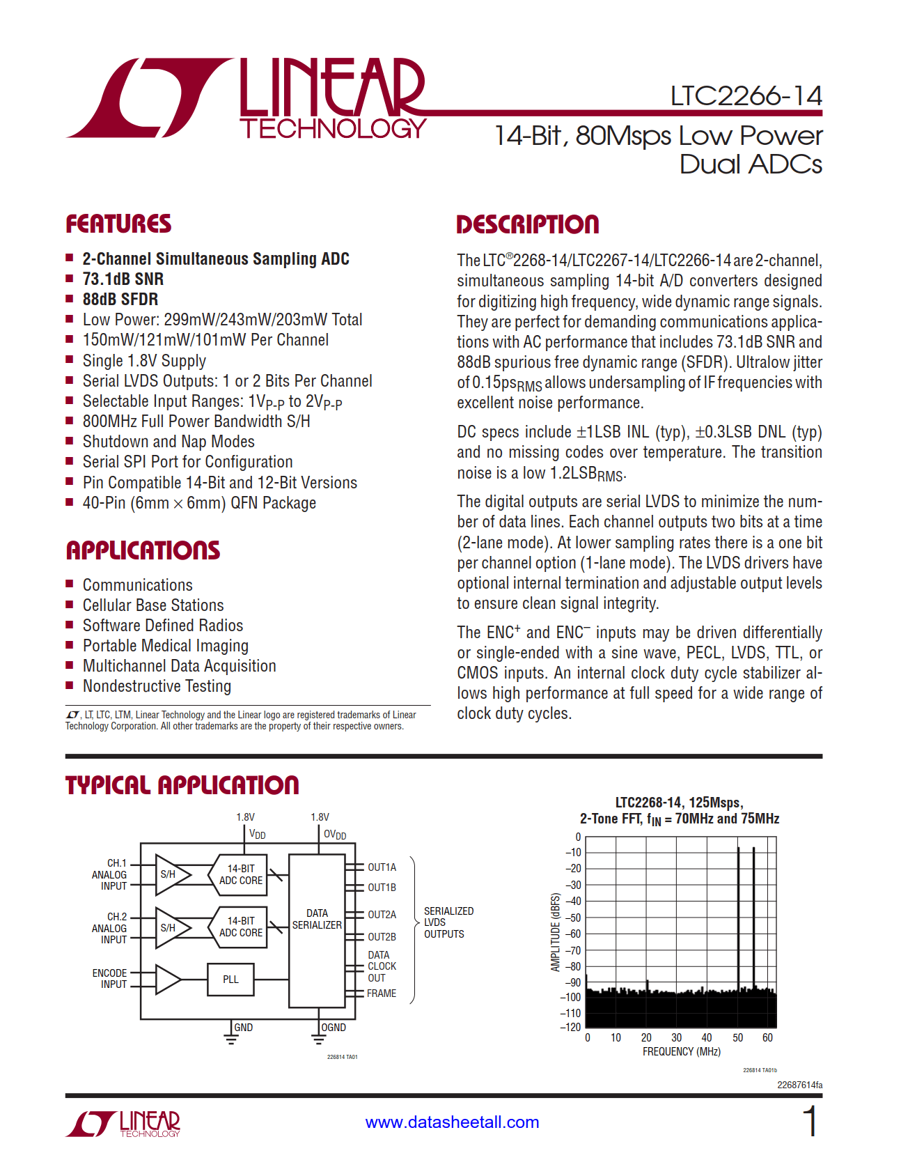
The LTC2266-14 are 2-channel, simultaneous sampling 14-bit A/D converters designed for digitizing high frequency, wide dynamic range signals. They are perfect for demanding communications applications with AC performance that includes 73.1dB SNR and 88dB spurious free dynamic range (SFDR). Ultralow jitter of 0.15psRMS allows undersampling of IF frequencies with excellent noise performance.
DC specs include ±1LSB INL (typ), ±0.3LSB DNL (typ) and no missing codes over temperature. The transition noise is a low 1.2LSBRMS.
The digital outputs are serial LVDS to minimize the number of data lines. Each channel outputs two bits at a time (2-lane mode). At lower sampling rates there is a one bit per channel option (1-lane mode). The LVDS drivers have optional internal termination and adjustable output levels to ensure clean signal integrity.
The ENC+ and ENC– inputs may be driven differentially or single-ended with a sine wave, PECL, LVDS, TTL, or CMOS inputs. An internal clock duty cycle stabilizer allows high performance at full speed for a wide range of clock duty cycles.