| Part No.: | ADP5054 |
| Page: | 31 Pages |
| Size: | 617 KB |
| Manufacturer: | Analog Devices, Inc. |
| Logo: |  |
| Views: | 1 |
| Update Time: | 2023-12-13 16:28:21 |
| DataSheet: | Download |
| Part No. | Packing | SPQ | Marking | MSL | Pins | Temp Range | Package Description | Buy |
| ADP5054ACPZ-R7 | Reel | 750 | 3 | 48 | -40°C ~ 125°C | 48-Lead Lead Frame Chip Scale Package [LFCSP] |
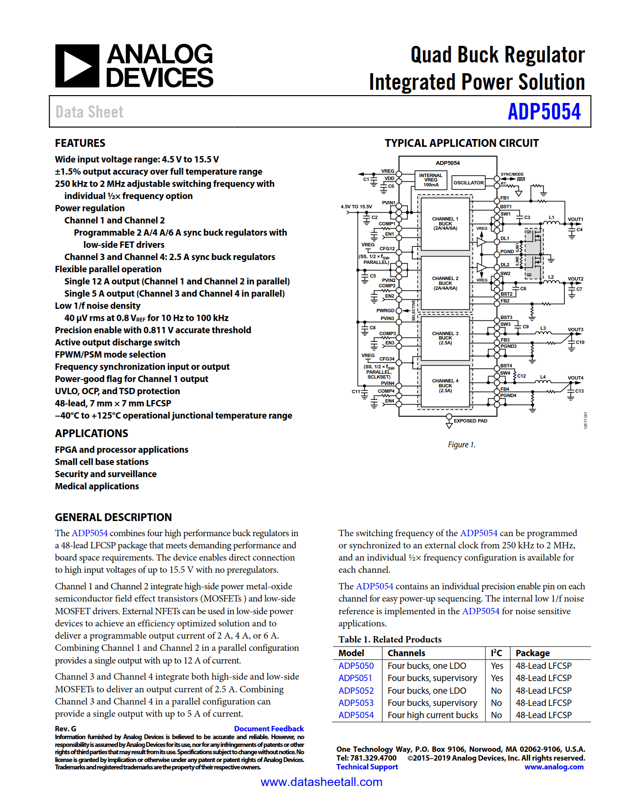
The ADP5054 combines four high performance buck regulators in a 48-lead LFCSP package that meets demanding performance and board space requirements. The device enables direct connection to high input voltages of up to 15.5 V with no preregulators.
Channel 1 and Channel 2 integrate high-side power metal-oxide semiconductor field effect transistors (MOSFETs) and low-side MOSFET drivers. External NFETs can be used in low-side power devices to achieve an efficiency optimized solution and to deliver a programmable output current of 2 A, 4 A, or 6 A. Combining Channel 1 and Channel 2 in a parallel configuration provides a single output with up to 12 A of current.
Channel 3 and Channel 4 integrate both high-side and low-side MOSFETs to deliver an output current of 2.5 A. Combining Channel 3 and Channel 4 in a parallel configuration can provide a single output with up to 5 A of current.
The switching frequency of the ADP5054 can be programmed or synchronized to an external clock from 250 kHz to 2 MHz, and an individual ½× frequency configuration is available for each channel.
The ADP5054 contains an individual precision enable pin on each channel for easy power-up sequencing. The internal low 1/f noise reference is implemented in the ADP5054 for noise sensitive applications.