| Part No.: | LTC2294 |
| Page: | 24 Pages |
| Size: | 665 KB |
| Manufacturer: | Linear Technology |
| Logo: |  |
| Views: | 2 |
| Update Time: | 2023-11-21 10:58:09 |
| DataSheet: | Download |
| Part No. | Packing | SPQ | Marking | MSL | Pins | Temp Range | Package Description | Buy |
| LTC2294IUP#PBF | Tube | 40 | LTC2294UP | 1 | 64 | -40°C ~ 85°C | 64-Lead QFN (9mm x 9mm x 0.75mm) | |
| LTC2294IUP#TRPBF | Reel | 2000 | LTC2294UP | 1 | 64 | -40°C ~ 85°C | 64-Lead QFN (9mm x 9mm x 0.75mm) | |
| LTC2294IUP#TRMPBF | Reel | 500 | LTC2294UP | 1 | 64 | -40°C ~ 85°C | 64-Lead QFN (9mm x 9mm x 0.75mm) | |
| LTC2294CUP#PBF | Tube | 40 | LTC2294UP | 1 | 64 | 0°C ~ 70°C | 64-Lead QFN (9mm x 9mm x 0.75mm) | |
| LTC2294CUP#TRPBF | Reel | 2000 | LTC2294UP | 1 | 64 | 0°C ~ 70°C | 64-Lead QFN (9mm x 9mm x 0.75mm) | |
| LTC2294CUP#TRMPBF | Reel | 500 | LTC2294UP | 1 | 64 | 0°C ~ 70°C | 64-Lead QFN (9mm x 9mm x 0.75mm) |
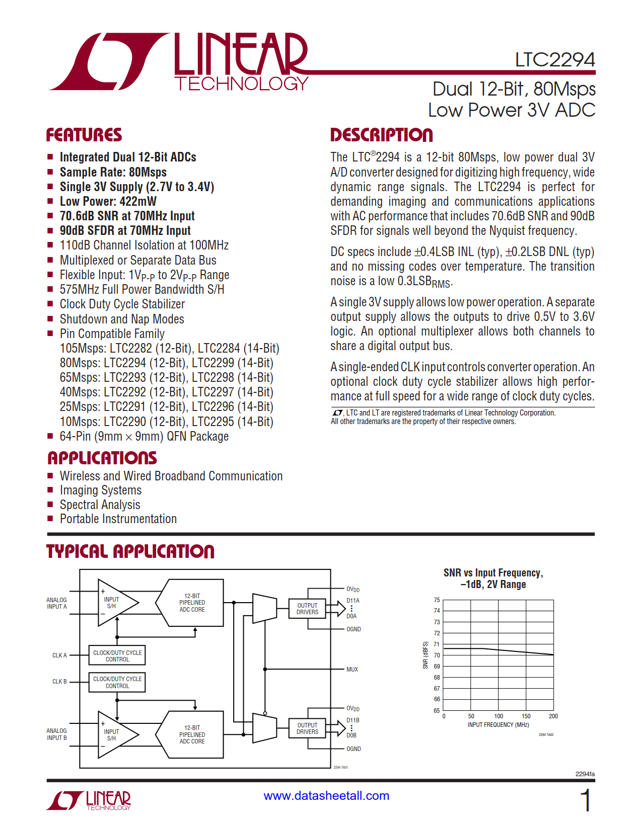
The LTC2294 is a 12-bit 80Msps, low power dual 3V A/D converter designed for digitizing high frequency, wide dynamic range signals. The LTC2294 is perfect for demanding imaging and communications applications with AC performance that includes 70.6dB SNR and 90dB SFDR for signals well beyond the Nyquist frequency.
DC specs include ±0.4LSB INL (typ), ±0.2LSB DNL (typ) and no missing codes over temperature. The transition noise is a low 0.3LSBRMS.
A single 3V supply allows low power operation. A separate output supply allows the outputs to drive 0.5V to 3.6V logic. An optional multiplexer allows both channels to share a digital output bus.
A single-ended CLK input controls converter operation. An optional clock duty cycle stabilizer allows high performance at full speed for a wide range of clock duty cycles.