| Part No.: | LTC2241-10 |
| Page: | 28 Pages |
| Size: | 474 KB |
| Manufacturer: | Linear Technology |
| Logo: |  |
| Views: | 1 |
| Update Time: | 2023-11-16 10:28:57 |
| DataSheet: | Download |
| Part No. | Packing | SPQ | Marking | MSL | Pins | Temp Range | Package Description | Buy |
| LTC2241CUP-10#PBF | Tube | 40 | LTC2241UP-10 | 1 | 64 | 0°C ~ 70°C | 64-Lead (9mm × 9mm) Plastic QFN | |
| LTC2241CUP-10#TRPBF | Reel | 2000 | LTC2241UP-10 | 1 | 64 | 0°C ~ 70°C | 64-Lead (9mm × 9mm) Plastic QFN | |
| LTC2241CUP-10#TRMPBF | Reel | 500 | LTC2241UP-10 | 1 | 64 | 0°C ~ 70°C | 64-Lead (9mm × 9mm) Plastic QFN | |
| LTC2241IUP-10#PBF | Tube | 40 | LTC2241UP-10 | 1 | 64 | -40°C ~ 85°C | 64-Lead (9mm × 9mm) Plastic QFN | |
| LTC2241IUP-10#TRPBF | Reel | 2000 | LTC2241UP-10 | 1 | 64 | -40°C ~ 85°C | 64-Lead (9mm × 9mm) Plastic QFN | |
| LTC2241IUP-10#TRMPBF | Reel | 500 | LTC2241UP-10 | 1 | 64 | -40°C ~ 85°C | 64-Lead (9mm × 9mm) Plastic QFN |
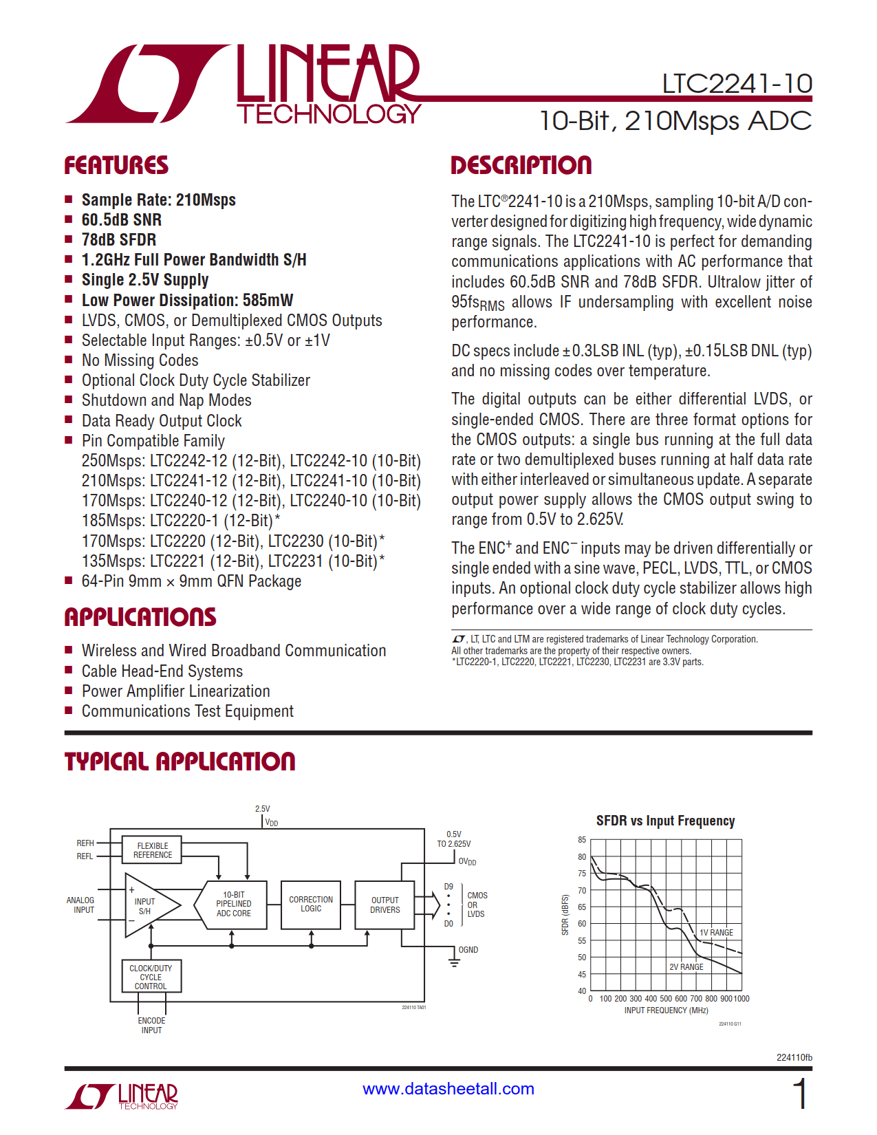
The LTC2241-10 is a 210Msps, sampling 10-bit A/D converter designed for digitizing high frequency, wide dynamic range signals. The LTC2241-10 is perfect for demanding communications applications with AC performance that includes 60.5dB SNR and 78dB SFDR. Ultralow jitter of 95fsRMS allows IF undersampling with excellent noise performance.
DC specs include ±0.3LSB INL (typ), ±0.15LSB DNL (typ) and no missing codes over temperature.
The digital outputs can be either differential LVDS, or single-ended CMOS. There are three format options for the CMOS outputs: a single bus running at the full data rate or two demultiplexed buses running at half data rate with either interleaved or simultaneous update. A separate output power supply allows the CMOS output swing to range from 0.5V to 2.625V.
The ENC+ and ENC– inputs may be driven differentially or single ended with a sine wave, PECL, LVDS, TTL, or CMOS inputs. An optional clock duty cycle stabilizer allows high performance over a wide range of clock duty cycles.