| Part No.: | LTC2220-1 |
| Page: | 28 Pages |
| Size: | 622 KB |
| Manufacturer: | Linear Technology |
| Logo: |  |
| Views: | 5 |
| Update Time: | 2023-11-15 15:37:49 |
| DataSheet: | Download |
| Part No. | Packing | SPQ | Marking | MSL | Pins | Temp Range | Package Description | Buy |
| LTC2220CUP-1#PBF | Tube | 40 | LTC2220UP-1 | 1 | 64 | 0°C ~ 70°C | 64-Lead QFN (9mm x 9mm x 0.75mm) | |
| LTC2220CUP-1#TRPBF | Reel | 2000 | LTC2220UP-1 | 1 | 64 | 0°C ~ 70°C | 64-Lead QFN (9mm x 9mm x 0.75mm) | |
| LTC2220CUP-1#TRMPBF | Reel | 500 | LTC2220UP-1 | 1 | 64 | 0°C ~ 70°C | 64-Lead QFN (9mm x 9mm x 0.75mm) | |
| LTC2220IUP-1#PBF | Tube | 40 | LTC2220UP-1 | 1 | 64 | -40°C ~ 85°C | 64-Lead QFN (9mm x 9mm x 0.75mm) | |
| LTC2220IUP-1#TRPBF | Reel | 2000 | LTC2220UP-1 | 1 | 64 | -40°C ~ 85°C | 64-Lead QFN (9mm x 9mm x 0.75mm) | |
| LTC2220IUP-1#TRMPBF | Reel | 500 | LTC2220UP-1 | 1 | 64 | -40°C ~ 85°C | 64-Lead QFN (9mm x 9mm x 0.75mm) |
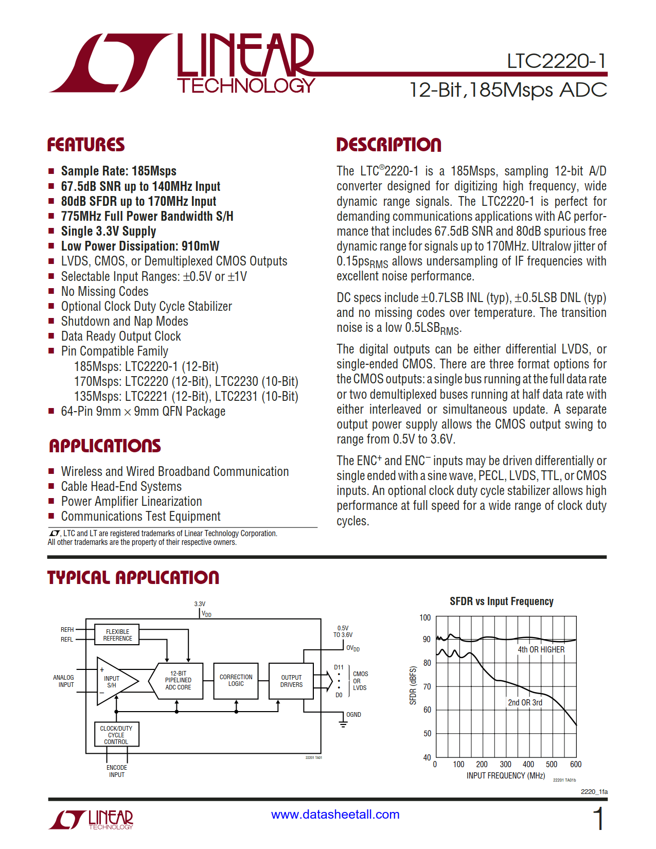
The LTC2220-1 is a 185Msps, sampling 12-bit A/D converter designed for digitizing high frequency, wide dynamic range signals. The LTC2220-1 is perfect for demanding communications applications with AC performance that includes 67.5dB SNR and 80dB spurious free dynamic range for signals up to 170MHz. Ultralow jitter of 0.15psRMS allows undersampling of IF frequencies with excellent noise performance.
DC specs include ±0.7LSB INL (typ), ±0.5LSB DNL (typ) and no missing codes over temperature. The transition noise is a low 0.5LSBRMS.
The digital outputs can be either differential LVDS, or single-ended CMOS. There are three format options for the CMOS outputs: a single bus running at the full data rate or two demultiplexed buses running at half data rate with either interleaved or simultaneous update. A separate output power supply allows the CMOS output swing to range from 0.5V to 3.6V.
The ENC+ and ENC- inputs may be driven differentially or single ended with a sine wave, PECL, LVDS, TTL, or CMOS inputs. An optional clock duty cycle stabilizer allows high performance at full speed for a wide range of clock duty cycles.