| Part No.: | LTC1750 |
| Page: | 20 Pages |
| Size: | 256 KB |
| Manufacturer: | Linear Technology |
| Logo: |  |
| Views: | 4 |
| Update Time: | 2023-11-14 11:23:33 |
| DataSheet: | Download |
| Part No. | Packing | SPQ | Marking | MSL | Pins | Temp Range | Package Description | Buy |
| LTC1750CFW#PBF | Tube | 39 | 1 | 48 | 0°C ~ 70°C | 48-Lead TSSOP | ||
| LTC1750CFW#TRPBF | Reel | 1800 | 1 | 48 | 0°C ~ 70°C | 48-Lead TSSOP | ||
| LTC1750CFW#TRMPBF | Reel | 500 | 1 | 48 | 0°C ~ 70°C | 48-Lead TSSOP | ||
| LTC1750IFW#PBF | Tube | 39 | 1 | 48 | -40°C ~ 85°C | 48-Lead TSSOP | ||
| LTC1750IFW#TRPBF | Reel | 1800 | 1 | 48 | -40°C ~ 85°C | 48-Lead TSSOP | ||
| LTC1750IFW#TRMPBF | Reel | 500 | 1 | 48 | -40°C ~ 85°C | 48-Lead TSSOP |
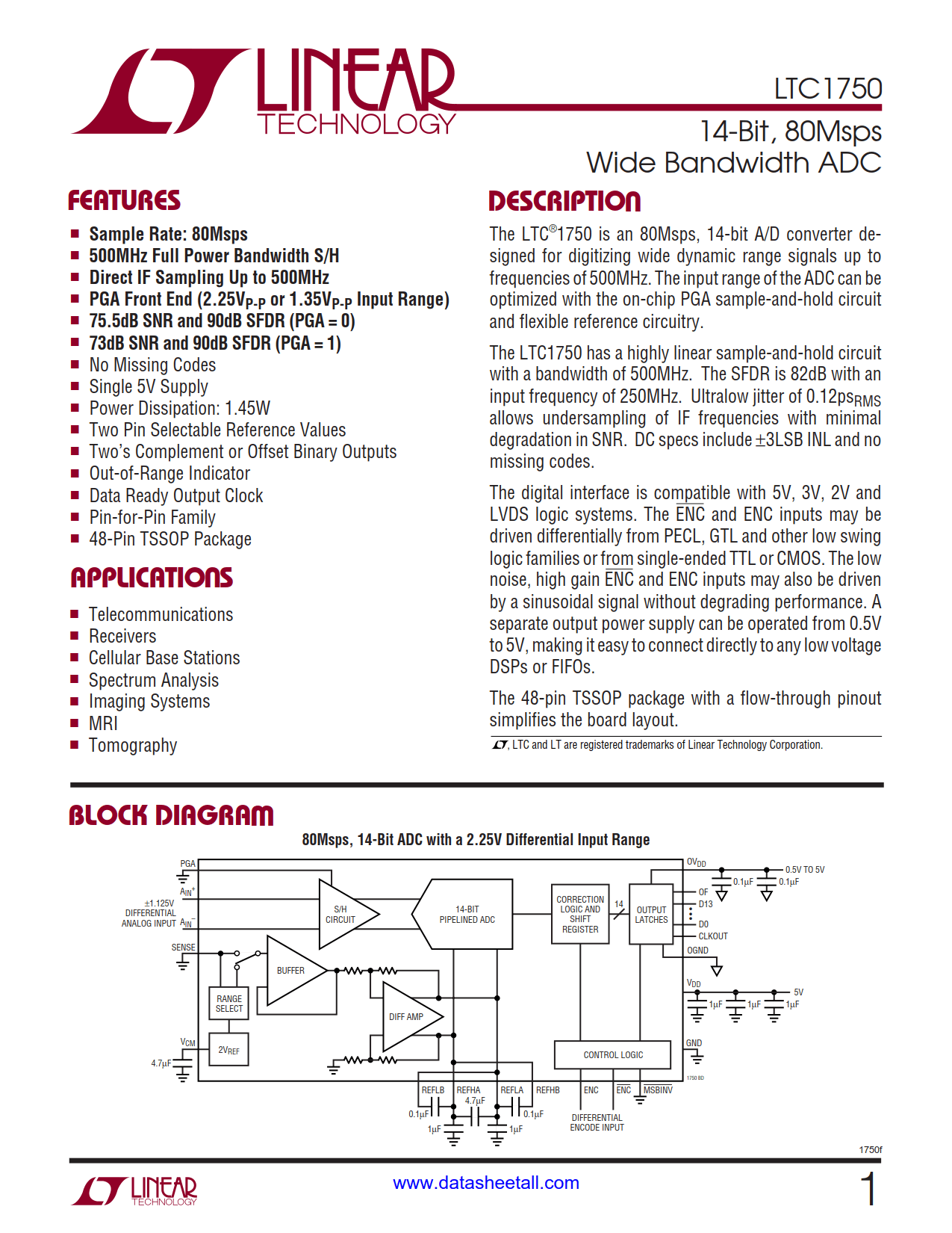
The LTC1750 is an 80Msps, 14-bit A/D converter designed for digitizing wide dynamic range signals up to frequencies of 500MHz. The input range of the ADC can be optimized with the on-chip PGA sample-and-hold circuit and flexible reference circuitry.
The LTC1750 has a highly linear sample-and-hold circuit with a bandwidth of 500MHz. The SFDR is 82dB with an input frequency of 250MHz. Ultralow jitter of 0.12psRMS allows undersampling of IF frequencies with minimal degradation in SNR. DC specs include ±3LSB INL and no missing codes.
The digital interface is compatible with 5V, 3V, 2V and LVDS logic systems. The ENC and ENC inputs may be driven differentially from PECL, GTL and other low swing logic families or from single-ended TTL or CMOS. The low noise, high gain ENC and ENC inputs may also be driven by a sinusoidal signal without degrading performance. A separate output power supply can be operated from 0.5V to 5V, making it easy to connect directly to any low voltage DSPs or FIFOs.
The 48-pin TSSOP package with a flow-through pinout simplifies the board layout.