| Part No.: | LTC1152 |
| Page: | 8 Pages |
| Size: | 206 KB |
| Manufacturer: | Linear Technology |
| Logo: |  |
| Views: | 1 |
| Update Time: | 2023-11-20 10:14:10 |
| DataSheet: | Download |
| Part No. | Packing | SPQ | Marking | MSL | Pins | Temp Range | Package Description | Buy |
| LTC1152CN8#PBF | Tube | 50 | 1152 | 1 | 8 | 0°C ~ 70°C | 8-Lead PDIP | |
| LTC1152CN8#TRPBF | Reel | 1152 | 1 | 8 | 0°C ~ 70°C | 8-Lead PDIP | ||
| LTC1152CN8#TRMPBF | Reel | 1152 | 1 | 8 | 0°C ~ 70°C | 8-Lead PDIP | ||
| LTC1152CS8#PBF | Tube | 100 | 1152 | 1 | 8 | 0°C ~ 70°C | 8-Lead SOIC | |
| LTC1152CS8#TRPBF | Reel | 2500 | 1152 | 1 | 8 | 0°C ~ 70°C | 8-Lead SOIC | |
| LTC1152CS8#TRMPBF | Reel | 500 | 1152 | 1 | 8 | 0°C ~ 70°C | 8-Lead SOIC | |
| LTC1152IN8#PBF | Tube | 50 | 1152I | 1 | 8 | -40°C ~ 85°C | 8-Lead PDIP | |
| LTC1152IN8#TRPBF | Reel | 1152I | 1 | 8 | -40°C ~ 85°C | 8-Lead PDIP | ||
| LTC1152IN8#TRMPBF | Reel | 1152I | 1 | 8 | -40°C ~ 85°C | 8-Lead PDIP | ||
| LTC1152IS8#PBF | Tube | 100 | 1152I | 1 | 8 | -40°C ~ 85°C | 8-Lead SOIC | |
| LTC1152IS8#TRPBF | Reel | 2500 | 1152I | 1 | 8 | -40°C ~ 85°C | 8-Lead SOIC | |
| LTC1152IS8#TRMPBF | Reel | 500 | 1152I | 1 | 8 | -40°C ~ 85°C | 8-Lead SOIC |
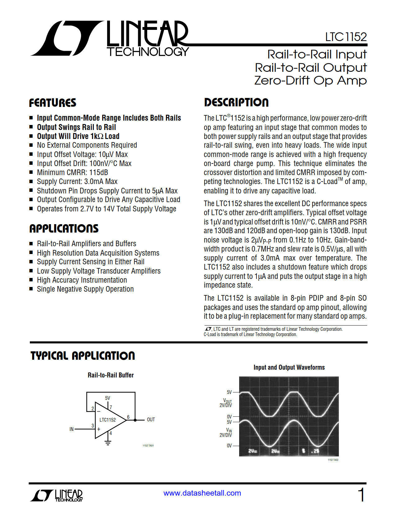
The LTC1152 is a high performance, low power zero-drift op amp featuring an input stage that common modes to both power supply rails and an output stage that provides rail-to-rail swing, even into heavy loads. The wide in put common-mode range is achieved with a high frequency on-board charge pump. This technique eliminates the crossover distortion and limited CMRR imposed by competing technologies. The LTC1152 is a C-Load™ op amp, enabling it to drive any capacitive load.
The LTC1152 shares the excellent DC performance specs of LTC’s other zero-drift amplifiers. Typical offset voltage is 1µVand typical off-set drift is 10nV/°C.CMRR and PSRR are 130dB and 120dB and open-loop gain is 130dB. Input noise voltage is 2µVP-P from 0.1Hz to 10Hz. Gain-bandwidth product is 0.7MHz and slew rate is 0.5V/µs, all with product is 0.7MHz and slew rate is 0.5V/µs, all with supply current of 3.0mA max over temperature. The LTC1152 also includes a shutdown feature which drops supply current to 1µA and puts the output stage in a high impedance state.
The LTC1152 is available in 8-pin PDIP and 8-pin SO packages and uses the standard op amp pin-out, allowing it to be a plug-in replacement for many standard op amps.