| Part No.: | LT3462A |
| Page: | 12 Pages |
| Size: | 431 KB |
| Manufacturer: | Linear Technology |
| Logo: |  |
| Views: | 1 |
| Update Time: | 2023-12-29 13:45:30 |
| DataSheet: | Download |
| Part No. | Packing | SPQ | Marking | MSL | Pins | Temp Range | Package Description | Buy |
| LT3462AES6#PBF | Tube | LTBGB | 1 | 6 | -40°C ~ 85°C | 6-Lead Plastic TSOT-23 | ||
| LT3462AES6#TRPBF | Reel | 2500 | LTBGB | 1 | 6 | -40°C ~ 85°C | 6-Lead Plastic TSOT-23 | |
| LT3462AES6#TRMPBF | Reel | 500 | LTBGB | 1 | 6 | -40°C ~ 85°C | 6-Lead Plastic TSOT-23 | |
| LT3462AEDC#PBF | Tube | LHGH | 1 | 8 | -40°C ~ 85°C | 8-Lead (2mm × 2mm) Plastic DFN | ||
| LT3462AEDC#TRPBF | Reel | 2500 | LHGH | 1 | 8 | -40°C ~ 85°C | 8-Lead (2mm × 2mm) Plastic DFN | |
| LT3462AEDC#TRMPBF | Reel | 500 | LHGH | 1 | 8 | -40°C ~ 85°C | 8-Lead (2mm × 2mm) Plastic DFN |
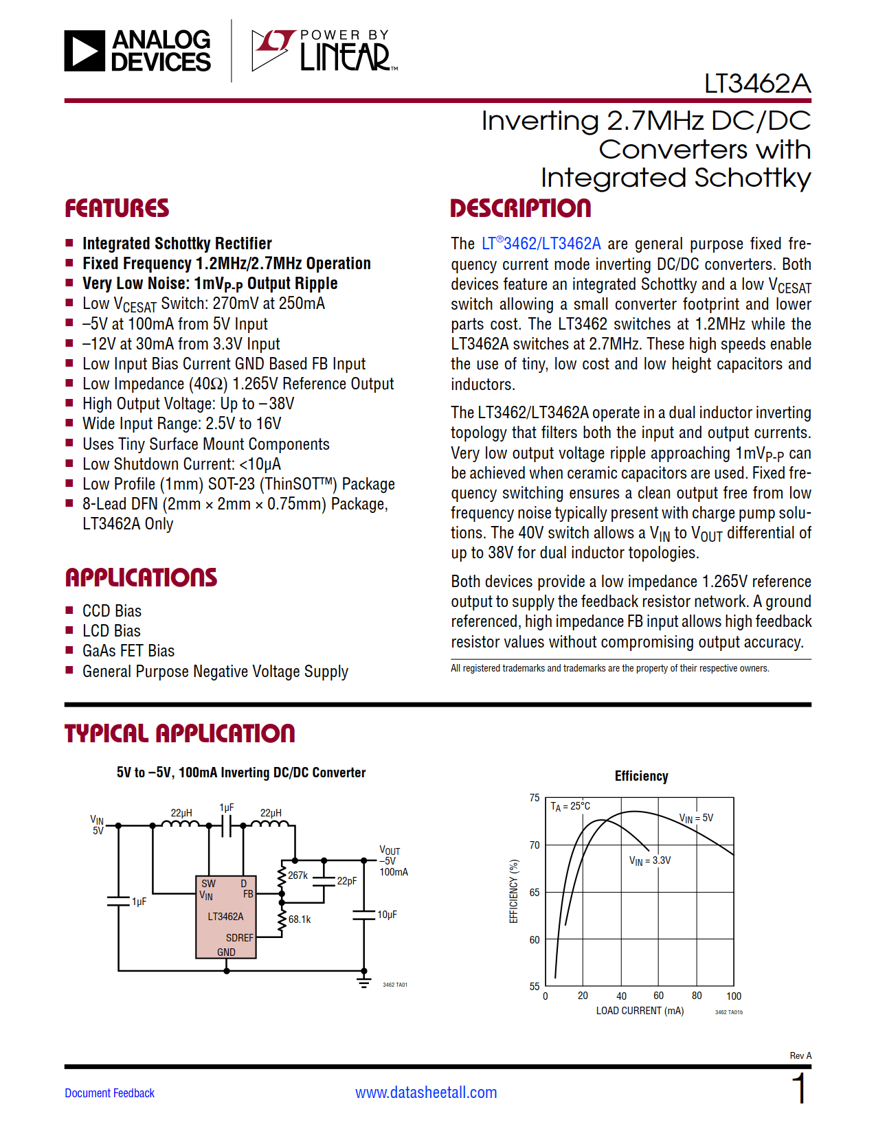
The LT3462A are general purpose fixed frequency current mode inverting DC/DC converters. Both devices feature an integrated Schottky and a low VCESAT switch allowing a small converter footprint and lower parts cost. The LT3462A switches at 2.7MHz. These high speeds enable the use of tiny, low cost and low height capacitors and inductors.
The LT3462A operate in a dual inductor inverting topology that filters both the input and output currents.Very low output voltage ripple approaching 1mVP-P can be achieved when ceramic capacitors are used. Fixed frequency switching ensures a clean output free from low frequency noise typically present with charge pump solutions.The 40V switch allows a VIN to VOUT differential ofup to 38V for dual inductor topologies.
Both devices provide a low impedance 1.265V reference output to supply the feedback resistor network. A ground referenced, high impedance FB input allows high feedback resistor values without compromising output accuracy.