| Part No.: | LT1130A |
| Page: | 12 Pages |
| Size: | 182 KB |
| Manufacturer: | Linear Technology |
| Logo: |  |
| Views: | 2 |
| Update Time: | 2024-12-18 11:31:49 |
| DataSheet: | Download |
| Part No. | Packing | SPQ | Marking | MSL | Pins | Temp Range | Package Description | Buy |
| LT1130ACNW#PBF | Tube | 14 | 1 | 28 | 0°C ~ 70°C | 28-Lead PDIP | ||
| LT1130ACSW#PBF | Tube | 27 | 1 | 28 | 0°C ~ 70°C | 28-Lead SOIC | ||
| LT1130ACSW#TRPBF | Reel | 1000 | 1 | 28 | 0°C ~ 70°C | 28-Lead SOIC | ||
| LT1130AISW#PBF | Tube | 27 | 1 | 28 | -40°C ~ 85°C | 28-Lead SOIC | ||
| LT1130AISW#TRPBF | Reel | 1000 | 1 | 28 | -40°C ~ 85°C | 28-Lead SOIC |
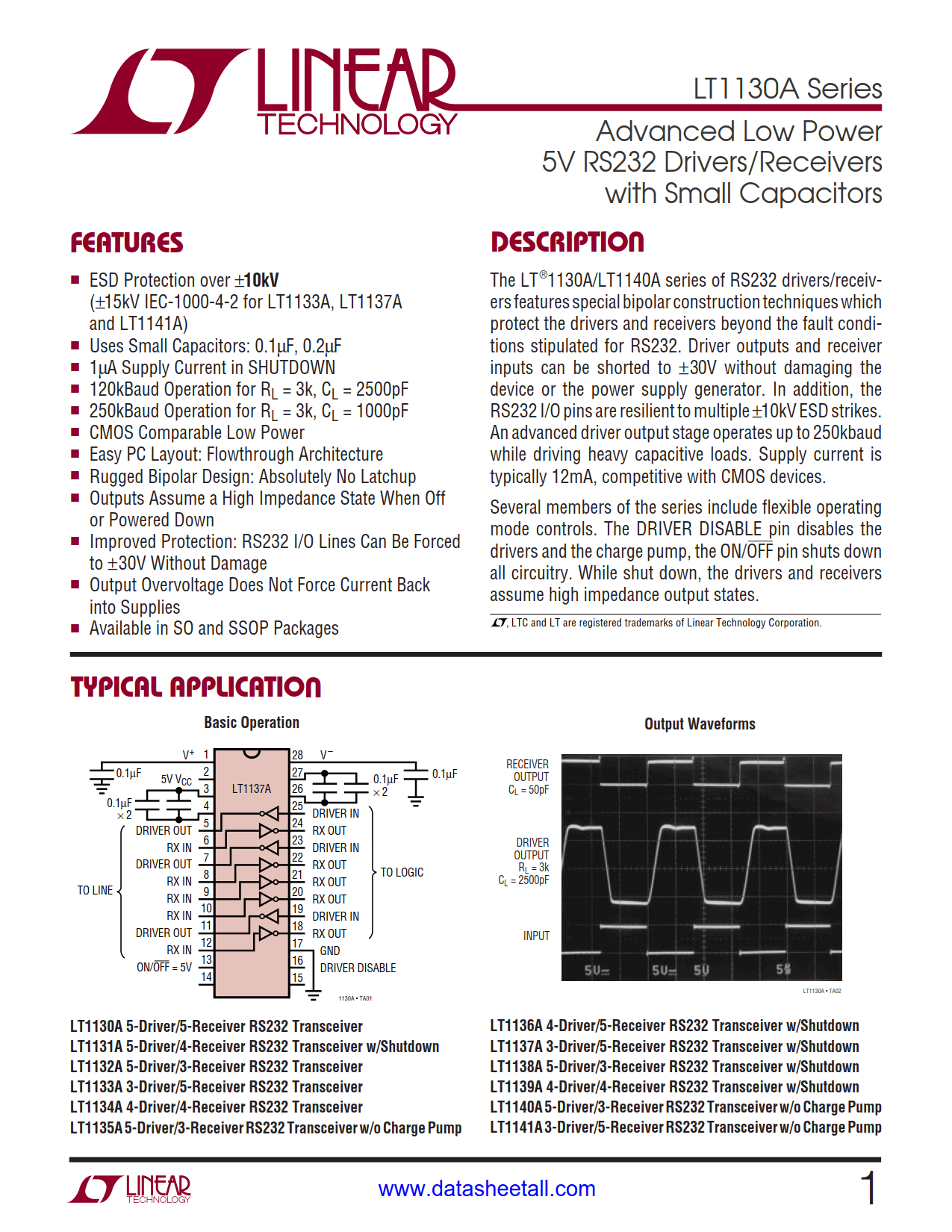
The LT1130A series of RS232 drivers/receivers features special bipolar construction techniques which protect the drivers and receivers beyond the fault conditions stipulated for RS232. Driver outputs and receiver inputs can be shorted to ±30V without damaging the device or the power supply generator. In addition, the RS232 I/O pins are resilient to multiple ±10kV ESD strikes. An advanced driver output stage operates up to 250kbaud while driving heavy capacitive loads. Supply current is typically 12mA, competitive with CMOS devices.
Several members of the series include flexible operating mode controls. The DRIVER DISABLE pin disables the drivers and the charge pump, the ON/OFF pin shuts down all circuitry. While shut down, the drivers and receivers assume high impedance output states.