| Part No.: | DAC8143 |
| Page: | 12 Pages |
| Size: | 190 KB |
| Manufacturer: | Analog Devices, Inc. |
| Logo: |  |
| Views: | 1 |
| Update Time: | 2023-12-20 10:27:35 |
| DataSheet: | Download |
| Part No. | Packing | SPQ | Marking | MSL | Pins | Temp Range | Package Description | Buy |
| DAC8143FP | 1 | 16 | -40°C ~ 85°C | 16-Lead Plastic DIP | ||||
| DAC8143FS | 1 | 16 | -40°C ~ 85°C | 16-Lead SOIC | ||||
| DAC8143FSZ-REEL | Reel | 1000 | 1 | 16 | -40°C ~ 85°C | 16-Lead SOIC Wide | ||
| DAC8143FPZ | Tube | 25 | 1 | 16 | -40°C ~ 85°C | 16-Lead PDIP | ||
| DAC8143FSZ | Tube | 47 | 1 | 16 | -40°C ~ 85°C | 16-Lead SOIC Wide |
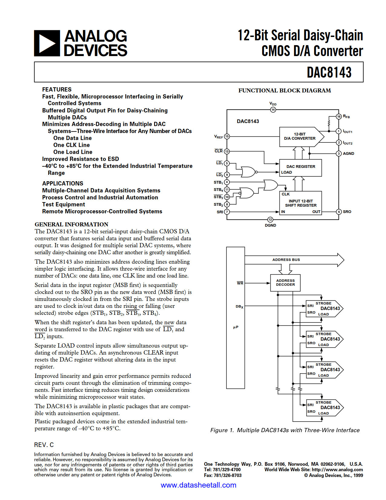
The DAC8143 is a 12-bit serial-input, daisy-chain digital-to-analog converter. It was designed for multiple serial DAC systems where serial daisy-chaining one DAC after another is greatly simplified. The daisy chain feature saves address-decoding lines enabling simpler logic interfacing in multiple package DAC designs.
The DAV8143 is ideal for data acquisition and process control systems offering the user a wide flexibility in output voltage ranges through choices of external references and output I-to-V converter op amps.
Serial data in the input register (MSB first) is sequentially clocked out to the SRO pin as the new data word (MSB first) is simultaneously clocked in from the SRI pin. The strobe inputs are used to clock in/out data on the rising or falling (user selected) strobe edges (STB1, STB2, STB3, STB4).
When the shift register’s data has been updated, the new data word is transferred to the DAC register with use of LD1 and LD2 inputs.
Separate LOAD control inputs allow simultaneous output updating of multiple DACs. An asynchronous CLEAR input resets the DAC register without altering data in the input register.
Improved linearity and gain error performance permits reduced circuit parts count through the elimination of trimming components. Fast interface timing reduces timing design considerations while minimizing microprocessor wait states.
The DAC8143 is available in plastic packages that are compatible with autoinsertion equipment.
Plastic packaged devices come in the extended industrial temperature range of –40°C to +85°C.