| Part No.: | ADF4382A |
| Page: | 70 Pages |
| Size: | 3724 KB |
| Manufacturer: | Analog Devices, Inc. |
| Logo: |  |
| Views: | 1 |
| Update Time: | 2024-01-12 10:14:06 |
| DataSheet: | Download |
| Part No. | Packing | SPQ | Marking | MSL | Pins | Temp Range | Package Description | Buy |
| ADF4382ABCCZ | Tray | 0 | 3 | 48 | -40°C ~ 105°C | 48-Terminal Land Grid Array [LGA] | ||
| ADF4382ABCCZ-RL7 | Reel | 500 | 3 | 48 | -40°C ~ 105°C | 48-Terminal Land Grid Array [LGA] |
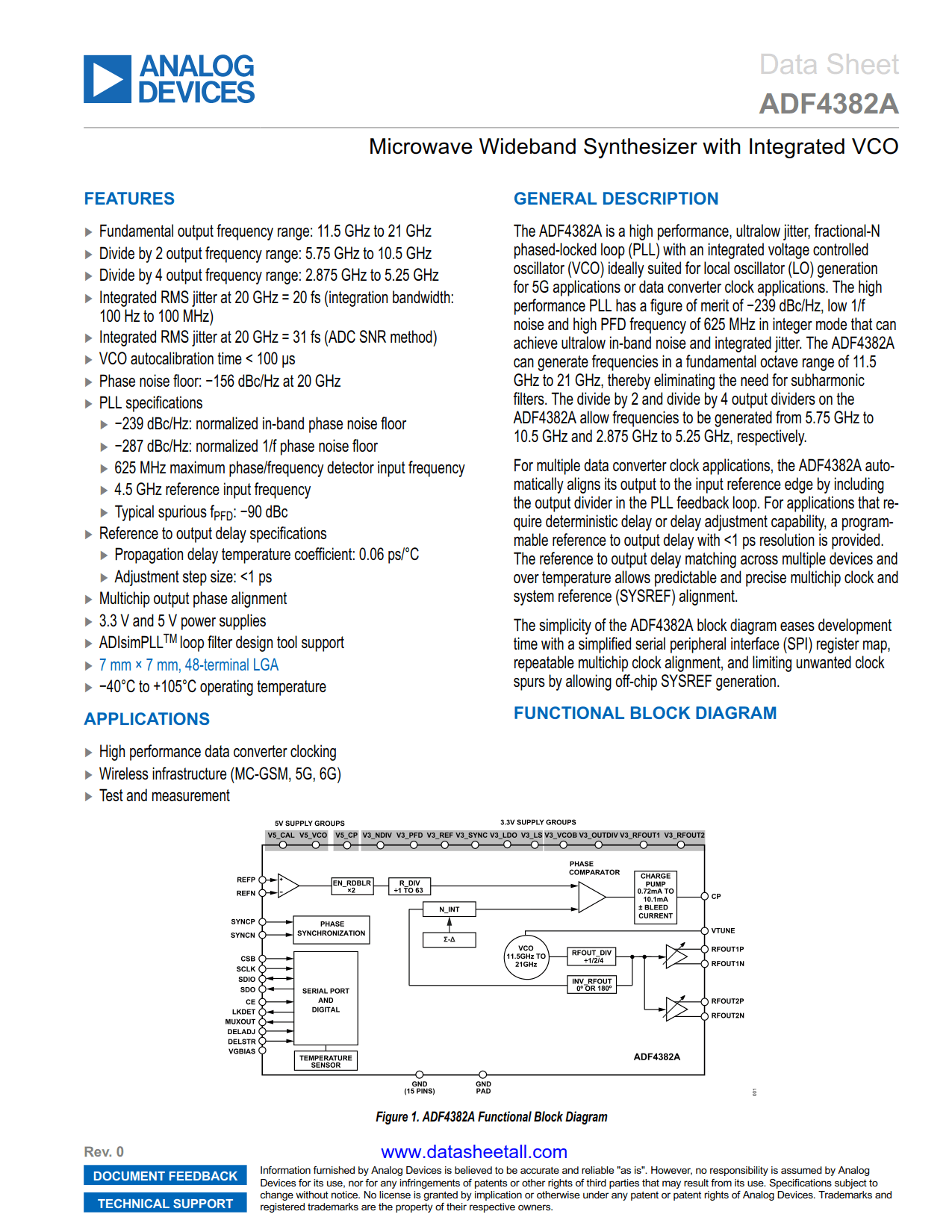
The ADF4382A is a high performance, ultralow jitter, fractional-N phased-locked loop (PLL) with an integrated voltage controlled oscillator (VCO) ideally suited for local oscillator (LO) generation for 5G applications or data converter clock applications. The high performance PLL has a figure of merit of −239 dBc/Hz, low 1/f noise and high PFD frequency of 625 MHz in integer mode that can achieve ultralow in-band noise and integrated jitter. The ADF4382A can generate frequencies in a fundamental octave range of 11.5 GHz to 21 GHz, thereby eliminating the need for subharmonic filters. The divide by 2 and divide by 4 output dividers on the ADF4382A allow frequencies to be generated from 5.75 GHz to 10.5 GHz and 2.875 GHz to 5.25 GHz, respectively.
For multiple data converter clock applications, the ADF4382A automatically aligns its output to the input reference edge by including the output divider in the PLL feedback loop. For applications that require deterministic delay or delay adjustment capability, a programmable reference to output delay with <1 ps resolution is provided. The reference to output delay matching across multiple devices and over temperature allows predictable and precise multichip clock and system reference (SYSREF) alignment.
The simplicity of the ADF4382A block diagram eases development time with a simplified serial peripheral interface (SPI) register map, repeatable multichip clock alignment, and limiting unwanted clock spurs by allowing off-chip SYSREF generation.