| Part No.: | ADA4351-2 |
| Page: | 36 Pages |
| Size: | 4227 KB |
| Manufacturer: | Analog Devices, Inc. |
| Logo: |  |
| Views: | 1 |
| Update Time: | 2024-01-12 10:27:12 |
| DataSheet: | Download |
| Part No. | Packing | SPQ | Marking | MSL | Pins | Temp Range | Package Description | Buy |
| ADA4351-2ACPZ | Tray | 714 | A50 | 1 | 16 | -40°C ~ 125°C | 16-Lead LFCSP (3mm x 3mm x 0.75mm) | |
| ADA4351-2ACPZ-R7 | Reel | 1500 | A50 | 1 | 16 | -40°C ~ 125°C | 16-Lead LFCSP (3mm x 3mm x 0.75mm) | |
| ADA4351-2ACPZ-RL | Reel | 5000 | A50 | 1 | 16 | -40°C ~ 125°C | 16-Lead LFCSP (3mm x 3mm x 0.75mm) |
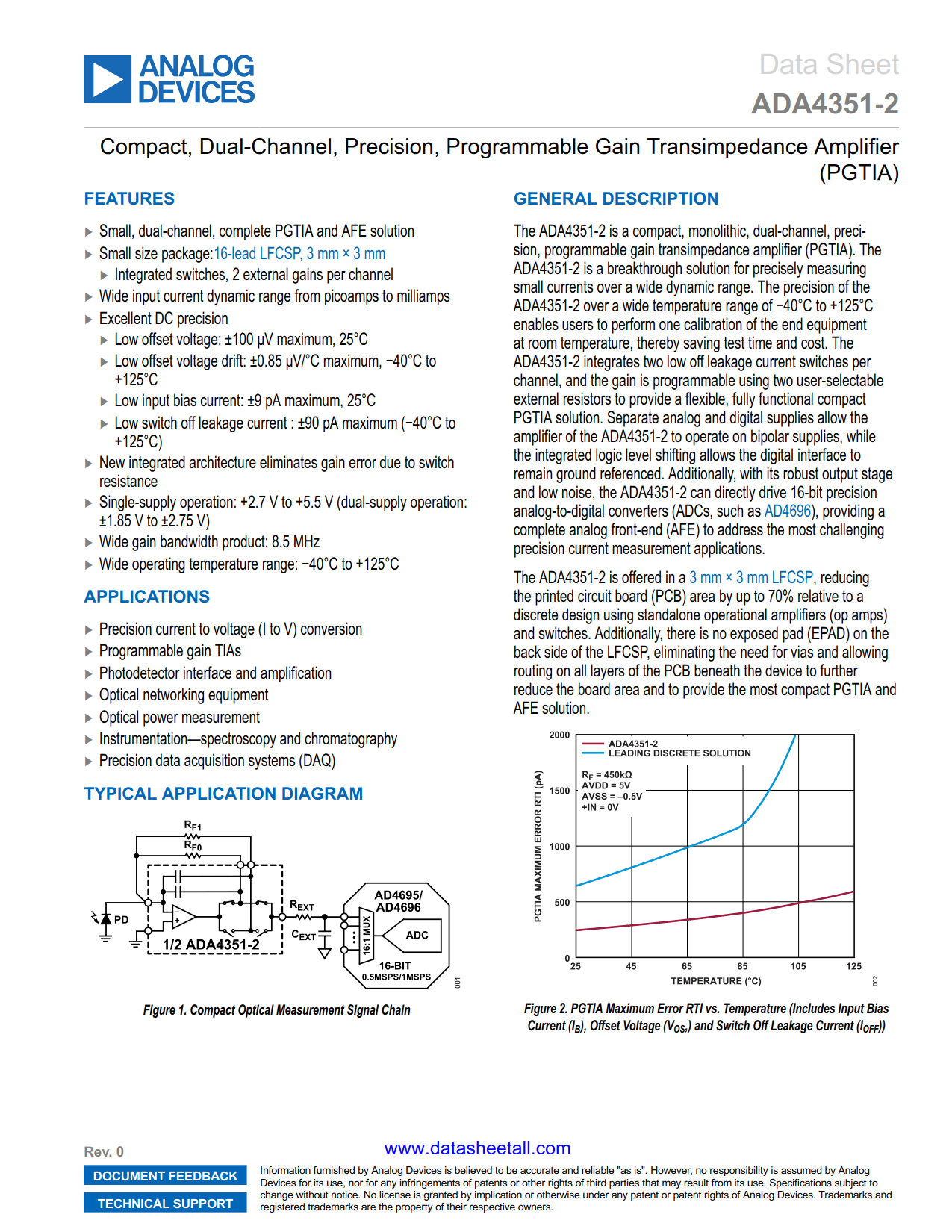
The ADA4351-2 is a compact, monolithic, dual-channel, precision, programmable gain transimpedance amplifier (PGTIA). The ADA4351-2 is a breakthrough solution for precisely measuring small currents over a wide dynamic range. The precision of the ADA4351-2 over a wide temperature range of −40°C to +125°C enables users to perform one calibration of the end equipment at room temperature, thereby saving test time and cost. The ADA4351-2 integrates two low off leakage current switches per channel, and the gain is programmable using two user-selectable external resistors to provide a flexible, fully functional compact PGTIA solution. Separate analog and digital supplies allow the amplifier of the ADA4351-2 to operate on bipolar supplies, while the integrated logic level shifting allows the digital interface to remain ground referenced. Additionally, with its robust output stage and low noise, the ADA4351-2 can directly drive 16-bit precision analog-to-digital converters (ADCs, such as AD4696), providing a complete analog front-end (AFE) to address the most challenging precision current measurement applications.
The ADA4351-2 is offered in a 3 mm × 3 mm LFCSP, reducing the printed circuit board (PCB) area by up to 70% relative to a discrete design using standalone operational amplifiers (op amps) and switches. Additionally, there is no exposed pad (EPAD) on the back side of the LFCSP, eliminating the need for vias and allowing routing on all layers of the PCB beneath the device to further reduce the board area and to provide the most compact PGTIA and AFE solution.