DataSheetAll » Manufacturer » Analog Devices, Inc. » AD9082 Datasheet
AD9082 Datasheet

AD9082 Datasheet

MxFE Quad, 16-Bit, 12 GSPS RF DAC and Dual, 12-Bit, 6 GSPS RF ADC
Part No.: AD9082
Page: 36 Pages
Size: 832 KB
Manufacturer: Analog Devices, Inc.
Logo:
Views: 1
Update Time: 2024-11-19 09:49:38
DataSheet: Download

AD9082 Datasheet Applicable Part

Part No. Packing SPQ Marking MSL Pins Temp Range Package Description Buy
AD9082BBPZ-4D2AC Tray 126   3 324 -40°C ~ 120°C 324-Ball BGA_ED (15mm x 15mm x 1.58mm)  
AD9082BBPZRL-4D2AC Reel 1000   3 324 -40°C ~ 120°C 324-Ball BGA_ED (15mm x 15mm x 1.58mm)  
AD9082BBPZ-2D2AC Tray 126   3 324 -40°C ~ 120°C 324-Ball BGA_ED (15mm x 15mm x 1.58mm)  
AD9082BBPZRL-2D2AC Reel 1000   3 324 -40°C ~ 120°C 324-Ball BGA_ED (15mm x 15mm x 1.58mm)  
SPQ:Standard Pack Quantity;MSL:Moisture Sensitivity Level

AD9082 Datasheet(PDF)

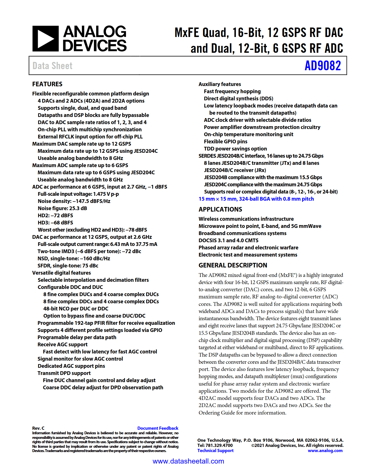
AD9082 Datasheet(Picture)

AD9082 Features

  • Flexible reconfigurable common platform design
    • 4 DACs and 2 ADCs (4D2A) and 2D2A options
    • Supports single, dual, and quad band
    • Datapaths and DSP blocks are fully bypassable
    • DAC to ADC sample rate ratios of 1, 2, 3, and 4
    • On-chip PLL with multichip synchronization
    • External RFCLK input option for off-chip PLL
  • Maximum DAC sample rate up to 12 GSPS
    • Maximum data rate up to 12 GSPS using JESD204C
    • Useable analog bandwidth to 8 GHz
  • Maximum ADC sample rate up to 6 GSPS
    • Maximum data rate up to 6 GSPS using JESD204C
    • Useable analog bandwidth to 8 GHz
  • ADC ac performance at 6 GSPS, input at 2.7 GHz, −1 dBFS
    • Full-scale input voltage: 1.475 V p-p
    • Noise density: −147.5 dBFS/Hz
    • Noise figure: 25.3 dB
    • HD2: −72 dBFS
    • HD3: −68 dBFS
    • Worst other (excluding HD2 and HD3): −78 dBFS
  • DAC ac performance at 12 GSPS, output at 2.6 GHz
    • Full-scale output current range: 6.43 mA to 37.75 mA
    • Two-tone IMD3 (−6 dBFS per tone): −72 dBc
    • NSD, single-tone: −160 dBc/Hz
    • SFDR, single-tone: 75 dBc
  • Versatile digital features
    • Selectable interpolation and decimation filters
    • Configurable DDC and DUC
      • 8 fine complex DUCs and 4 coarse complex DUCs
      • 8 fine complex DDCs and 4 coarse complex DDCs
      • 48-bit NCO per DUC or DDC
      • Option to bypass fine and coarse DUC/DDC
    • Programmable 192-tap PFIR filter for receive equalization
    • Supports 4 different profile settings loaded via GPIO
    • Programable delay per data path
    • Receive AGC support
      • Fast detect with low latency for fast AGC control
    • Signal monitor for slow AGC control
    • Dedicated AGC support pins
    • Transmit DPD support
      • Fine DUC channel gain control and delay adjust
      • Coarse DDC delay adjust for DPD observation path
  • Auxiliary features
    • Fast frequency hopping
    • Direct digital synthesis (DDS)
    • Low latency loopback modes (receive datapath data can be routed to the transmit datapaths)
    • ADC clock driver with selectable divide ratios
    • Power amplifier downstream protection circuitry
    • On-chip temperature monitoring unit
    • Flexible GPIO pins
    • TDD power savings option
  • SERDES JESD204B/JESD204C interface, 16 lanes up to 24.75 Gbps
    • 8 lanes JESD204B/C transmitter (JT×) and 8 lanes
    • JESD204B/C receiver (JR×)
    • JESD204B compliance with the maximum 15.5 Gbps
    • JESD204C compliance with the maximum 24.75 Gbps
    • Supports real or complex digital data (8-, 12-, 16-, or 24-bit)
  • 15 mm × 15 mm, 324-ball BGA with 0.8 mm pitch

AD9082 Applications

  • Wireless communications infrastructure
  • Microwave point-to-point, E-band and 5G mmWave
  • Broadband communications systems
  • DOCSIS 3.1 and 4.0 CMTS
  • Phased array radar and electronic warfare
  • Electronic test and measurement systems

AD9082 Description

The AD9082 mixed signal front-end (MxFE®) is a highly integrated device with a 16-bit, 12 GSPS maximum sample rate, RF digital-to-analog converter (DAC) core, and 12-bit, 6 GSPS maximum sample rate, RF analog-to-digital converter (ADC) cores. The AD9082 is well suited for applications requiring both wideband ADCs and DACs to process signal(s) having wide instantaneous bandwidth. The device features eight transmit lanes and eight receive lanes that support 24.75 Gbps/lane JESD204C or 15.5 Gbps/lane JESD204B standards. The device also has an on-chip clock multiplier and digital signal processing (DSP) capability targeted at either wideband or multiband, direct to RF applications. The DSP datapaths can be bypassed to allow a direct connection between the converter cores and the JESD204B/C data transceiver port. The device also features low latency loopback, frequency hopping modes, and datapath multiplexer (mux) configurations useful for phase array radar system and electronic warfare applications. Two models for the AD9082 are offered.

The 4D2AC model supports four DACs and two ADCs. The 2D2AC model supports two DACs and two ADCs.
AD9082 Datasheet Related Parts

About DataSheetAll|Contact Us|Privacy Policy|Manufacturer List|Sitemap|XML|TXT
CopyRight © 2024 DataSheetAll(datasheetall.com)