| Part No.: | AD5940 |
| Page: | 134 Pages |
| Size: | 1991 KB |
| Manufacturer: | Analog Devices, Inc. |
| Logo: |  |
| Views: | 2 |
| Update Time: | 2024-01-10 14:55:44 |
| DataSheet: | Download |
| Part No. | Packing | SPQ | Marking | MSL | Pins | Temp Range | Package Description | Buy |
| AD5940BCBZ-RL | Reel | 5000 | 1 | 56 | -40°C ~ 85°C | 56-Ball WLCSP (4.16 mm x 3.56 mm) | ||
| AD5940BCBZ-RL7 | Reel | 1500 | 1 | 56 | -40°C ~ 85°C | 56-Ball WLCSP (4.16 mm x 3.56 mm) |
The AD5940 are high precision, low power analog front ends (AFEs) designed for portable applications that require high precision, electrochemical-based measurement techniques, such as amperometric, voltammetric, or impedance measurements. The AD5940 is designed for skin impedance and body impedance measurements, and works with the AD8233 AFE in a complete bioelectric or biopotential measurement system. The AD5940 is designed for electrochemical toxic gas sensing.
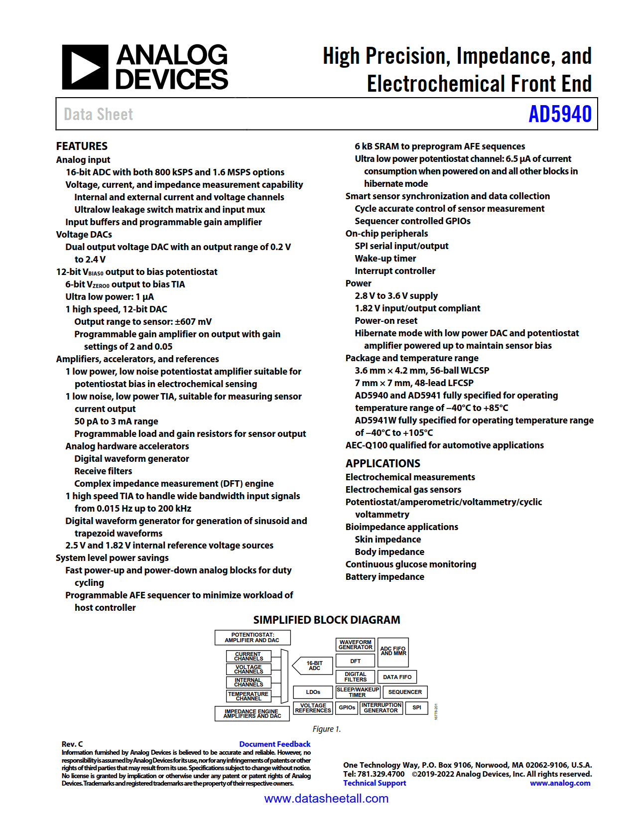
The AD5940 consist of two high precision excitation loops and one common measurement channel, which enables a wide capability of measurements of the sensor under test. The first excitation loop consists of an ultra low power, dual-output string, digital-to-analog converter (DAC), and a low power, low noise potentiostat. One output of the DAC controls the noninverting input of the potentiostat, and the other output controls the noninverting input of the transimpedance amplifier (TIA). This low power excitation loop is capable of generating signals from dc to 200 Hz.
The second excitation loop consists of a 12-bit DAC, referred to as the high speed DAC. This DAC is capable of generating high frequency excitation signals up to 200 kHz.
The AD5940 measurement channel features a 16-bit, 800 kSPS, multichannel successive approximation register (SAR) analog-to-digital converter (ADC) with input buffers, a built in antialias filter, and a programmable gain amplifier (PGA). An input multiplexer (mux) in front of the ADC allows the user to select an input channel for measurement. These input channels include multiple external current inputs, external voltage inputs, and internal channels. The internal channels allow diagnostic measurements of the internal supply voltages, die temperature, and reference voltages.
The current inputs include two TIAs with programmable gain and load resistors for measuring different sensor types. The first TIA, referred to as the low power TIA, measures low bandwidth signals. The second TIA, referred to as the high speed TIA, measures high bandwidth signals up to 200 kHz.
An ultra low leakage, programmable switch matrix connects the sensor to the internal analog excitation and measurement blocks. This matrix provides an interface for connecting external transimpedance amplifier resistors (RTIAs) and calibration resistors. The matrix can also be used to multiplex multiple electronic measurement devices to the same wearable electrodes.
A precision 1.82 V and 2.5 V on-chip reference source is available. The internal ADC and DAC circuits use this on-chip reference source to ensure low drift performance for the 1.82 V and 2.5 V peripherals.
The AD5940 measurement blocks can be controlled via direct register writes through the serial peripheral interface (SPI) interface, or, alternatively, by using a preprogrammable sequencer, which provides autonomous control of the AFE chip. 6 kB of static random access memory (SRAM) is partitioned for a deep data first in, first out (FIFO) and command FIFO. Measurement commands are stored in the command FIFO and measurement results are stored in the data FIFO. A number of FIFO related interrupts are available to indicate when the FIFO is full.
A number of general-purpose inputs/outputs (GPIOs) are available and controlled using the AFE sequencer. The AFE sequencer allows cycle accurate control of multiple external sensor devices.
The AD5940 operate from a 2.8 V to 3.6 V supply and are specified over a temperature range of −40°C to +85°C. The AD5940 is packaged in a 56-lead, 3.6 mm × 4.2 mm WLCSP.