| Part No.: | AD4856 |
| Page: | 68 Pages |
| Size: | 2676 KB |
| Manufacturer: | Analog Devices, Inc. |
| Logo: |  |
| Views: | 2 |
| Update Time: | 2025-01-13 21:23:39 |
| DataSheet: | Download |
| Part No. | Packing | SPQ | Marking | MSL | Pins | Temp Range | Package Description | Buy |
| AD4856BBCZ | Tube | 416 | 3 | 64 | -40°C ~ 125°C | 64-Lead BGA (7mm × 7mm × 1.42mm) | ||
| AD4856BBCZ-RL-13 | Reel | 2000 | 3 | 64 | -40°C ~ 125°C | 64-Lead BGA (7mm × 7mm × 1.42mm) |
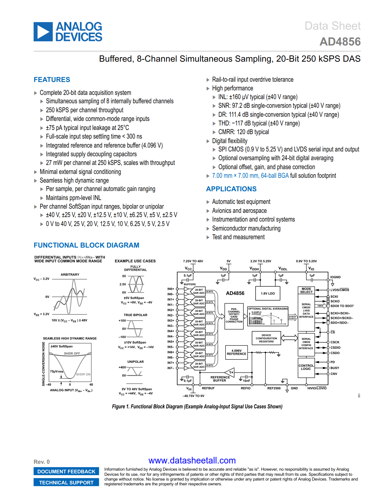
The AD4856 is a fully buffered, 8-channel simultaneous sampling, 20-bit, 250 kSPS data acquisition system (DAS) with differential, wide common-mode range inputs. Its functional architecture is shown in Figure 1. Operating from a 5 V low voltage supply, flexible input buffer supplies, and using the precision low drift internal reference and reference buffer, the AD4856 allows the SoftSpan range of each channel to be independently configured to match the native application signal swing, minimizing additional external signal conditioning. To further maximize single-conversion dynamic range, the AD4856 incorporates seamless high dynamic range (SHDR) technology. When enabled, the input signal path gain of the channel is automatically optimized on a sample-by-sample basis, minimizing converter noise on each sample without impacting linearity.
The 11 MHz bandwidth, picoamp input analog buffers, wide input common-mode range, and 120 dB common-mode rejection ratio (CMRR) of the AD4856 allow the DAS to directly digitize input signals with arbitrary swings on INx+ and INx−. Its input signal flexibility, combined with ±160 μV integral nonlinearity (INL), no missing codes at 20 bits, 97.2 dB signal to noise ratio (SNR), and 111.4 dB dynamic range, make the AD4856 an ideal choice for applications requiring high accuracy, throughput, and precision in a compact solution footprint. Enabling 24-bit oversampling offers further SNR and dynamic range improvements. Optional per channel offset, gain, and phase adjustment provide the ability to calibrate and remove system-level errors upstream to the DAS.
The AD4856 features a serial peripheral interface (SPI) register configuration bus (0.9 V to 5.25 V) and supports both low voltage differential signaling buses (LVDS) and complementary metal-oxide semiconductor (CMOS) conversion data output buses, selectable using the LVDS/CMOS pin. Between one and eight lines of data output can be employed in CMOS mode, allowing the user to optimize bus width and throughput.
The 7.00 mm × 7.00 mm, 64-ball, ball grid array (BGA) of the AD4856 includes all critical power supply and reference bypass capacitors, minimizing full solution footprint and component count and reducing sensitivity to application printed circuit board (PCB) layout. The device operates over an extended industrial temperature range of −40°C to +125°C.
Note that throughout this data sheet, multifunction pins such as LVDS/CMOS are referred to either by the entire pin name or by a single function of the pin. For example, LVDS when only that function is relevant.